- 您现在的位置:买卖IC网 > Sheet目录3887 > PIC16F84A-20E/SS (Microchip Technology)IC MCU CMOS 20MHZ 1K FLSH 20SSOP
PIC16F84A
DS35007B-page 4
2001 Microchip Technology Inc.
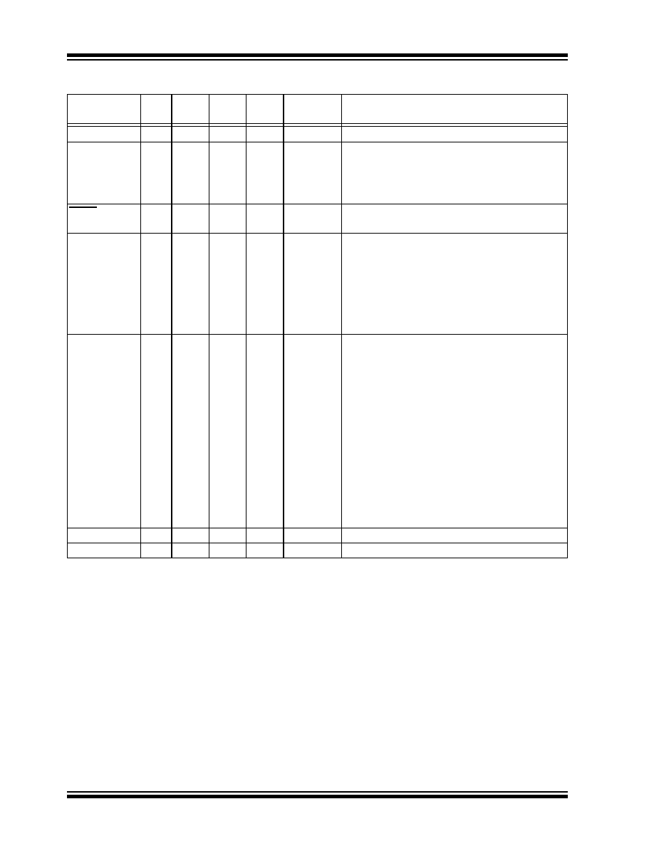
TABLE 1-1:
PIC16F84A PINOUT DESCRIPTION
Pin Name
PDIP
No.
SOIC
No.
SSOP
No.
I/O/P
Type
Buffer
Type
Description
OSC1/CLKIN
16
18
I
ST/CMOS(3) Oscillator crystal input/external clock source input.
OSC2/CLKOUT
15
19
O
—
Oscillator crystal output. Connects to crystal or
resonator in Crystal Oscillator mode. In RC mode,
OSC2 pin outputs CLKOUT, which has 1/4 the
frequency of OSC1 and denotes the instruction
cycle rate.
MCLR
4
I/P
ST
Master Clear (Reset) input/programming voltage
input. This pin is an active low RESET to the device.
PORTA is a bi-directional I/O port.
RA0
17
19
I/O
TTL
RA1
18
20
I/O
TTL
RA2
1
I/O
TTL
RA3
2
I/O
TTL
RA4/T0CKI
3
I/O
ST
Can also be selected to be the clock input to the
TMR0 timer/counter. Output is open drain type.
PORTB is a bi-directional I/O port. PORTB can be
software programmed for internal weak pull-up on
all inputs.
RB0/INT
6
7
I/O
TTL/ST(1)
RB0/INT can also be selected as an external
interrupt pin.
RB1
7
8
I/O
TTL
RB2
8
9
I/O
TTL
RB3
9
10
I/O
TTL
RB4
10
11
I/O
TTL
Interrupt-on-change pin.
RB5
11
12
I/O
TTL
Interrupt-on-change pin.
RB6
12
13
I/O
TTL/ST(2)
Interrupt-on-change pin.
Serial programming clock.
RB7
13
14
I/O
TTL/ST(2)
Interrupt-on-change pin.
Serial programming data.
VSS
5
5,6
P
—
Ground reference for logic and I/O pins.
VDD
14
15,16
P
—
Positive supply for logic and I/O pins.
Legend: I= input
O = Output
I/O = Input/Output
P = Power
— = Not used
TTL = TTL input
ST = Schmitt Trigger input
Note 1: This buffer is a Schmitt Trigger input when configured as the external interrupt.
2: This buffer is a Schmitt Trigger input when used in Serial Programming mode.
3: This buffer is a Schmitt Trigger input when configured in RC oscillator mode and a CMOS input otherwise.
发布紧急采购,3分钟左右您将得到回复。
相关PDF资料
22-15-3113
CONN FFC/FPC 11POS .100 RT ANG
22-02-3113
CONN FFC/FPC VERTICAL 11POS .100
PIC16F84A-20E/SO
IC MCU CMOS 20MHZ 1K FLSH 18SOIC
PIC16F84A-04E/SS
IC MCU CMOS 4MHZ 1K FLASH 20SSOP
PIC16F84A-04E/SO
IC MCU CMOS 4MHZ 1K FLASH 18SOIC
PIC16F785-I/SS
IC PIC MCU FLASH 2KX14 20SSOP
PIC16C433T-I/SO
IC MCU CMOS 8BIT 10MHZ 2K 18SOIC
PIC16C773T-E/SO
IC MCU OTP 4KX14 A/D PWM 28SOIC
相关代理商/技术参数
PIC16F84A-20I/P
功能描述:8位微控制器 -MCU 1.75KB 68 RAM 13 I/O 20MHz IndTemp PDIP18 RoHS:否 制造商:Silicon Labs 核心:8051 处理器系列:C8051F39x 数据总线宽度:8 bit 最大时钟频率:50 MHz 程序存储器大小:16 KB 数据 RAM 大小:1 KB 片上 ADC:Yes 工作电源电压:1.8 V to 3.6 V 工作温度范围:- 40 C to + 105 C 封装 / 箱体:QFN-20 安装风格:SMD/SMT
PIC16F84A-20I/P
制造商:Microchip Technology Inc 功能描述:IC 8BIT FLASH MCU 16F84 DIP18
PIC16F84A-20I/SO
功能描述:8位微控制器 -MCU 1.75KB 68 RAM 13 I/O 20MHz IndTemp SOIC18 RoHS:否 制造商:Silicon Labs 核心:8051 处理器系列:C8051F39x 数据总线宽度:8 bit 最大时钟频率:50 MHz 程序存储器大小:16 KB 数据 RAM 大小:1 KB 片上 ADC:Yes 工作电源电压:1.8 V to 3.6 V 工作温度范围:- 40 C to + 105 C 封装 / 箱体:QFN-20 安装风格:SMD/SMT
PIC16F84A-20I/SO
制造商:Microchip Technology Inc 功能描述:8BIT FLASH MCU SMD 16F84 SOIC18
PIC16F84A-20I/SS
功能描述:8位微控制器 -MCU 1.75KB 68 RAM 13 I/O 20MHz IndTemp SSOP20 RoHS:否 制造商:Silicon Labs 核心:8051 处理器系列:C8051F39x 数据总线宽度:8 bit 最大时钟频率:50 MHz 程序存储器大小:16 KB 数据 RAM 大小:1 KB 片上 ADC:Yes 工作电源电压:1.8 V to 3.6 V 工作温度范围:- 40 C to + 105 C 封装 / 箱体:QFN-20 安装风格:SMD/SMT
PIC16F84A-20I/SS
制造商:Microchip Technology Inc 功能描述:8BIT FLASH MCU SMD 16F84 SSOP20
PIC16F84A-20I/SS
制造商:Microchip Technology Inc 功能描述:Microcontroller IC Number of I/Os:13
PIC16F84AT-04/SO
功能描述:8位微控制器 -MCU 1.75KB 68 RAM 13 I/O 4MHz SOIC18 RoHS:否 制造商:Silicon Labs 核心:8051 处理器系列:C8051F39x 数据总线宽度:8 bit 最大时钟频率:50 MHz 程序存储器大小:16 KB 数据 RAM 大小:1 KB 片上 ADC:Yes 工作电源电压:1.8 V to 3.6 V 工作温度范围:- 40 C to + 105 C 封装 / 箱体:QFN-20 安装风格:SMD/SMT